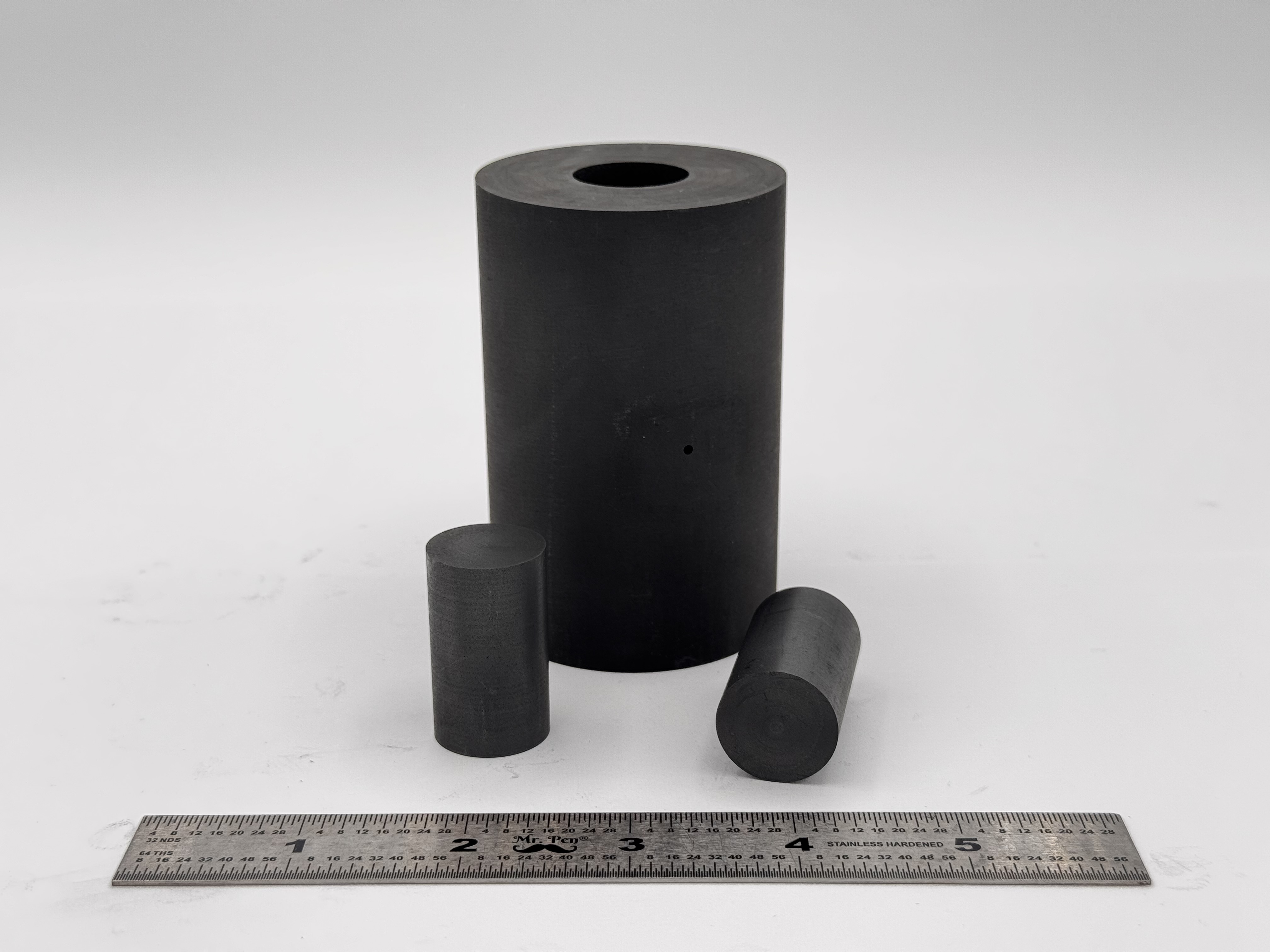
 High Strength SPS Graphite Tooling
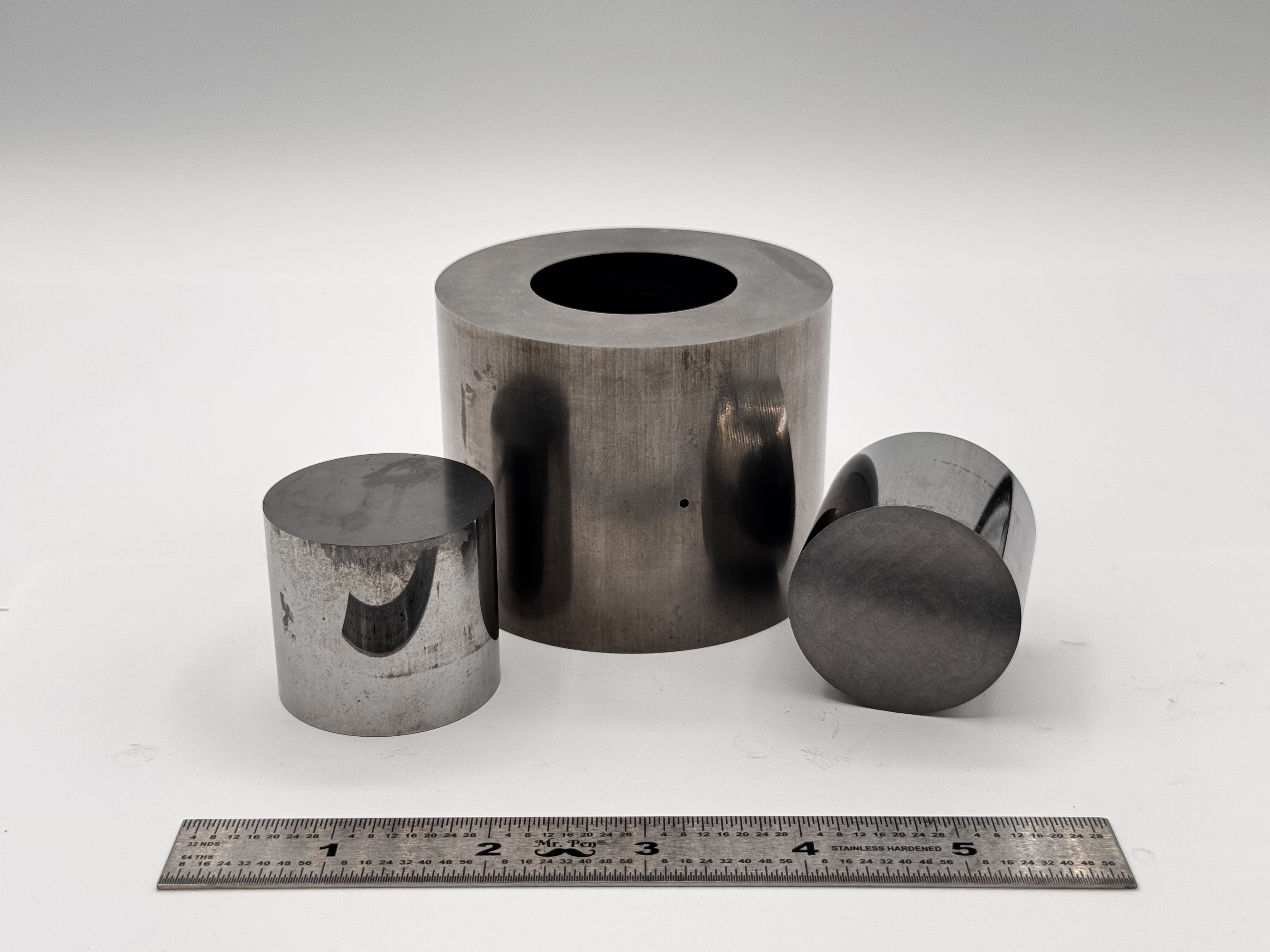 Tungsten Carbide Tooling
 Carbon Graphite Foil / Paper
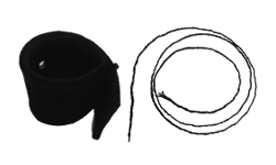 Carbon Felt and Yarn
 Spark Plasma Sintering Systems
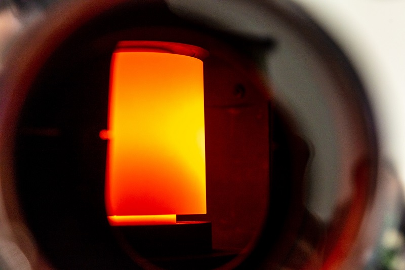 SPS/FAST Modeling Software
Revolutionizing Material Science: Spark Plasma Sintering Systems
In the rapidly evolving world of material science, California Nanotechnologies stands at the forefront with its cutting-edge Spark Plasma Sintering (SPS) systems. These advanced machines are transforming the way powdered materials are consolidated into dense, solid forms, paving the way for innovations across various industries.
What is Spark Plasma Sintering?
Spark Plasma Sintering is an advanced sintering technology that uses the combination of pulsed electrical currents and mechanical pressure to rapidly heat and densify powdered materials. This process results in high-density materials with superior properties, all achieved at lower temperatures and shorter times compared to traditional sintering methods.
The SPS Process: How It Works
The SPS process begins with placing the raw powdered material into a high-temperature-resistant die, typically made of graphite. High-energy electrical pulses are then applied, creating sparks between the powder particles. These sparks generate localized heating, facilitating particle bonding and reducing porosity. Simultaneously, mechanical pressure is applied, ensuring the material is densely packed. This entire process occurs in a controlled environment, often a vacuum or inert gas atmosphere, to prevent oxidation and contamination.
Advantages of Spark Plasma Sintering
California Nanotechnologies’ SPS systems offer several significant advantages:
- Rapid Sintering: Achieve full densification in a fraction of the time compared to conventional methods, thanks to the efficient heat transfer from the electrical pulses.
- Fine-Grained Microstructure: Retain the fine-grained structure of the starting powders, resulting in materials with enhanced mechanical properties.
- Versatility: Process a wide range of materials, including metals, ceramics, composites, and functionally graded materials.
- Energy Efficiency: Reduce overall energy consumption with localized heating, making the process more sustainable and cost-effective.
Applications Across Industries
The applications of SPS technology are vast and varied, driving innovation in numerous fields:
- Advanced Ceramics: Produce dense, high-performance ceramic components for aerospace, electronics, and biomedical applications.
- Hard Metals: Manufacture cutting tools and wear-resistant parts with improved hardness and toughness.
- Functional Materials: Develop materials with specific electrical, magnetic, or thermal properties for use in sensors, actuators, and electronic devices.
- Nanostructured Materials: Fabricate materials with nanoscale features, enhancing their mechanical and functional properties.
California Nanotechnologies: Leading the Charge
California Nanotechnologies is dedicated to pushing the boundaries of what’s possible with SPS technology. Our SPS systems are designed with precision and innovation, offering unmatched performance and reliability. We collaborate with leading researchers and industries to develop tailored solutions that meet the unique needs of our clients.
By investing in an SPS system from California Nanotechnologies, you are not only adopting a state-of-the-art technology but also partnering with a company committed to excellence and advancement in material science.
Transform Your Materials with California Nanotechnologies
Whether you are in aerospace, electronics, biomedical, or any other industry relying on advanced materials, California Nanotechnologies' Spark Plasma Sintering systems can help you achieve new heights of performance and innovation. Contact us today to learn more about how our SPS systems can revolutionize your materials processing capabilities.