SEM Analysis
Cal Nano, offers Scanning Electron Microscopy (SEM) services along with Energy Dispersive Spectroscopy (EDS) and Electron Backscatter Diffraction (EBSD), which serve as invaluable tools for material and product development. SEM is a high-resolution imaging technique that allows for detailed examination of a material's surface morphology, topography, and microstructure. By partnering with academic institutions and industry leaders, Cal Nano can provide access to state-of-the-art SEM equipment, enabling researchers and engineers to analyze materials at the micro- and nanoscale levels.
In addition to SEM imaging, Cal Nano offers EDS and EBSD analysis as part of their services. EDS provides elemental analysis, identifying the chemical composition of a sample based on the characteristic X-ray emissions generated by the interaction of the sample with the electron beam. This information is crucial for understanding the elemental distribution within a material, identifying impurities, and evaluating the chemical integrity of products during development. EBSD analysis enables researchers to study crystal orientations, grain boundaries, and phase identification, offering insights into the mechanical properties and performance of materials
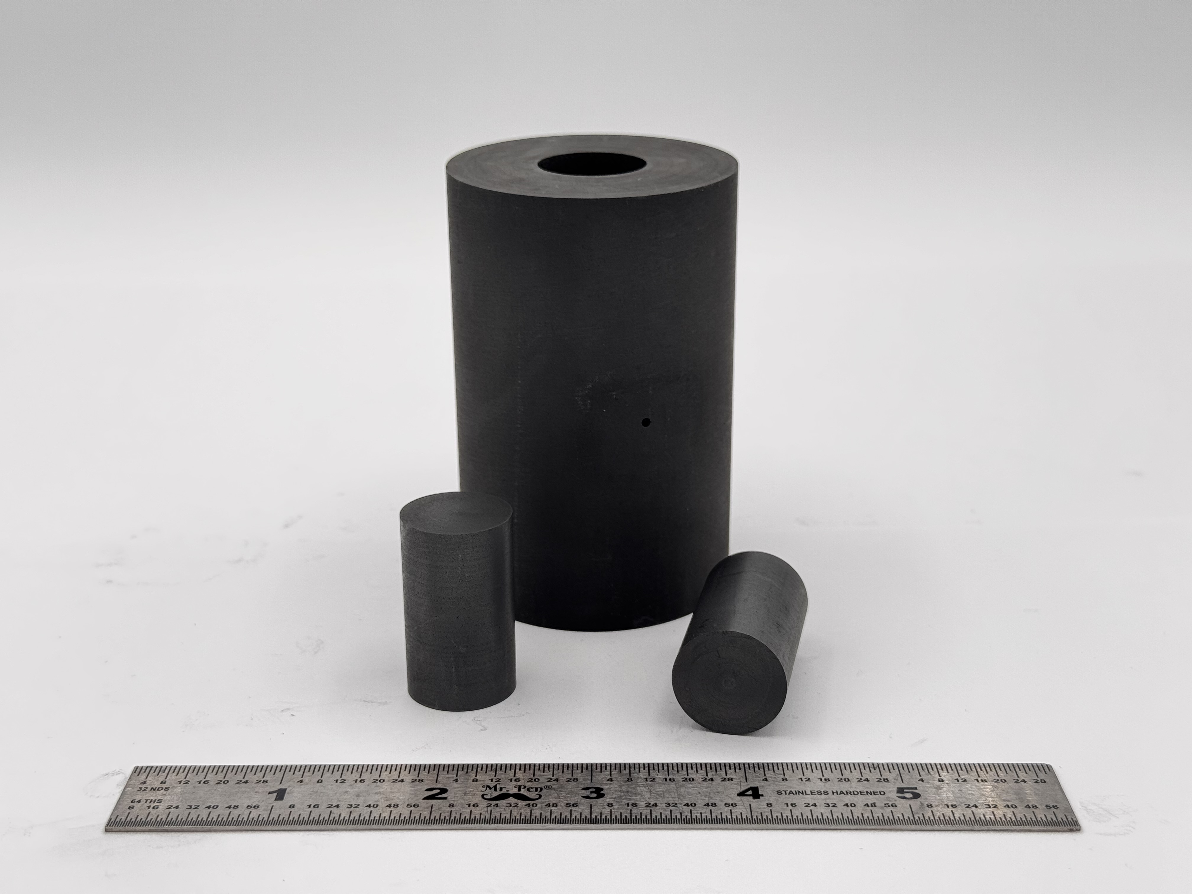
 High Strength SPS Graphite Tooling
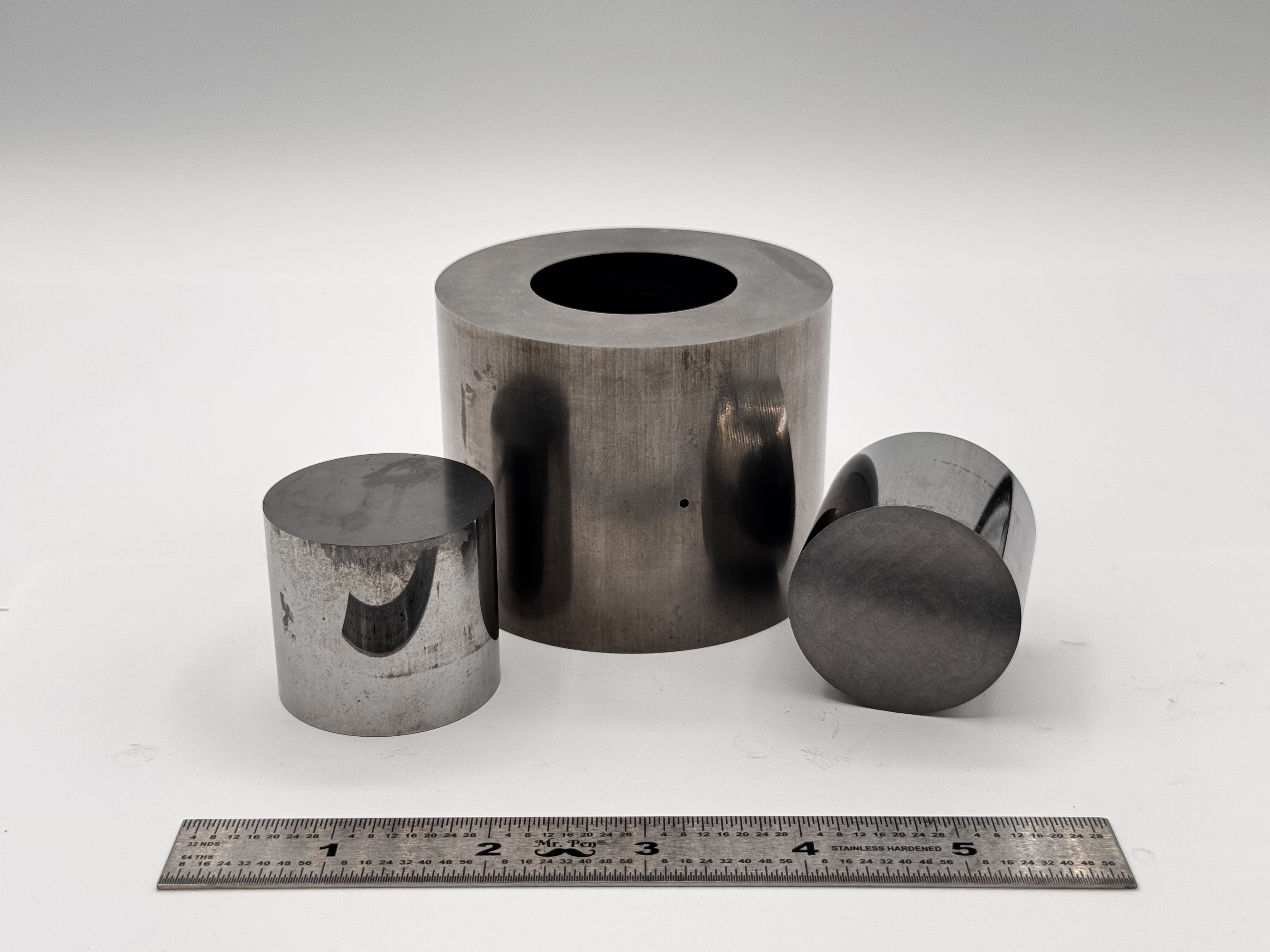
 Tungsten Carbide Tooling
 Carbon Graphite Foil / Paper
 Carbon Felt and Yarn
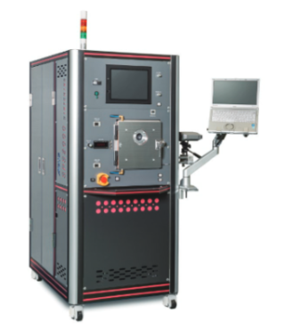
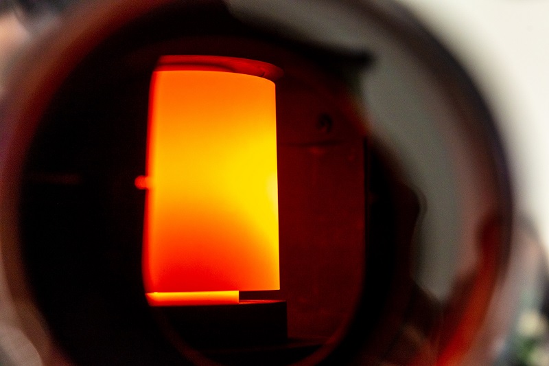
 Spark Plasma Sintering Systems
 SPS/FAST Modeling Software